Diodes, Diode Circuits, and Applications
The following concepts build off of the content taught in "L0: Charge Doping". Make sure to cover all of this material if you are new to diodes, specifically with understanding P-type and N-type silicon. We will start with the introduction of the PN junction which forms the essence of what a diode really is.
The PN Junction
As we know from the previous lecture, Silicon is not a very good conductor intrinsically. Thus, we need to dope it in order to increase its conductivity. Recall that with P-Type silicon impurities were added to the silicon in order to add holes into the material that would allow more electrons to be accepted (ie. increasing conductivity). N-Type silicon would add more free electrons to increase the conductivity.
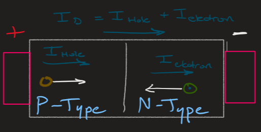
A beautiful thing happens when P-type silicon is place next to N-type silicon. We form what is known as a "PN Junction", we call the Junction or region between the two type of silicon the Depletion Region. A diode internally is composed of ohmic metal leads connected to a P-Type silicon next to a N-Type silicon. The reason I mention the ohmic metal leads is because this will have a large affect when we flow large amounts of current though these diodes. When the diode is "forward biased", or when the voltage difference from the P-Type to the N-Type (we call this voltage Vd) is positive and greater than the threshold voltage a current will start to flow from the high potential to the low potential. This current that flows across the diode has the symbol Id
A beautiful thing happens when P-type silicon is place next to N-type silicon. We form what is known as a "PN Junction", we call the Junction or region between the two type of silicon the Depletion Region. A diode internally is composed of ohmic metal leads connected to a P-Type silicon next to a N-Type silicon. The reason I mention the ohmic metal leads is because this will have a large affect when we flow large amounts of current though these diodes. When the diode is "forward biased", or when the voltage difference from the P-Type to the N-Type (we call this voltage Vd) is positive and greater than the threshold voltage a current will start to flow from the high potential to the low potential. This current that flows across the diode has the symbol Id
Id = Iholes + Ielectrons
- Iholes is the current that comes from the movement of holes from the P-type material to the N-type material. The holes take the form of protons so since their charge is positive and their current is in the direction of conventional current flow, this current is positive.
- Ielectrons is the current that comes from the movement of the electrons from the N-type material to the P-type material. The electrons have a negative charge and since their direction of movement is in the opposite direction to current flow, these two negatives make a positive current.
- Iholes ~Ielectrons if the amount of N-type doping equals the amount of P-type doing. If not, the abundant carrier will have more current flow.
I-V Characteristics
Now that we understand how current flows across the PN junction we can move on to understanding the I-V graph of the diode.
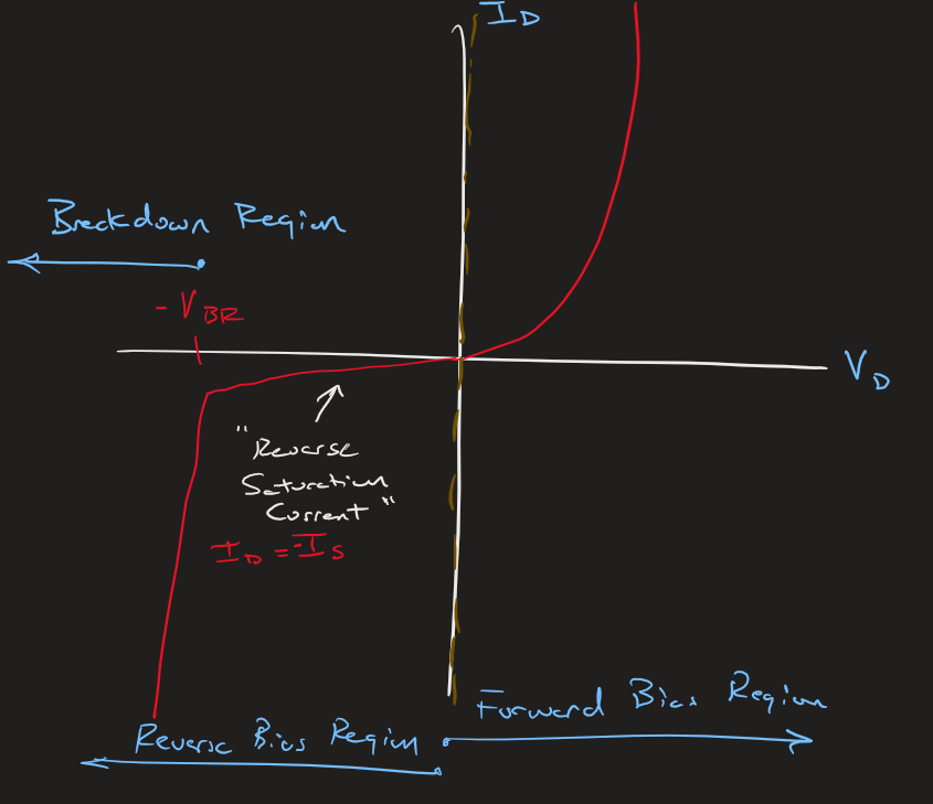
As seen from the graph above, there exist 3 regions of operation for the diode. From what we have seen so far, when the Vd is positive the diode is in the Forward Bias Region. While this is a basic model of a diode, real diodes will have a required forward voltage (VTH) that needs to be reached before current will be able to move across the junction. When looking at the graph above we can see the interesting part of the diode which is during negative Vd region which we call the Reverse Bias Region. Within the reverse bias region, at voltages between zero and the breakdown voltage the current that moves across the diode remains almost constant at a value known as the Reverse Saturation Current Is. A sub-region within the reverse bias region is for voltages less than the Breakdown Voltage represented as the symbol VBR. This Breakdown Voltage is also a function of the amount of doping in the junction (ie. more doping results in a smaller Voltage breakdown value). It is past this breakdown voltage to which the voltage is high enough to ionize the depletion region and allow large amounts of current to flow in the reverse direction, this phenomena is known as a Zener Breakdown.
From the I-V graph seen above it is obvious that this graph is not linear as seen with the past electrical components we had seen. This is because diodes are characterized as non-linear devices. This can make things a bit more tricky... but as you will see, we will create different models of the diode to figure out what the voltage and current characteristics of the diode are.
The Diode Non-Linear Model
We will look at many models that can be used to represent diodes. The following model is however the most accurate in representing the non-linear behavior of a diode. The equation we will be using is known as the Shockley Diode Equation:
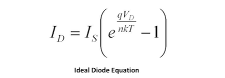
- Is is the Saturation Current of the Diode, representing the current magnitude when reversed bias greater than the breakdown voltage
- q is the Elementary Charge constant = 1.602 x 10^-19 [Coulombs]
- VD is the voltage drop across the diode
- n is the ideality factor of the diode which is a value near 1.0 based on the quality of the diode (ie. how close it is to an ideal diode)
- k is Boltzmann's constant = 1.3806 x 10^-23 [Joules/Kelvin]
- T is the Temperature of the Diode in Kelvin, which for most scenarios we will use room temperature (300.16 K)
- It is also important to note that k * T / q = VT where VT is known as the Thermal Voltage
When looking at the Foward Bias Region of the diode since the change in current value goes from 1nA to 1uA to 1mA within a small voltage difference, using a logarithmic scale for the current axis is very helpful! Look at this:
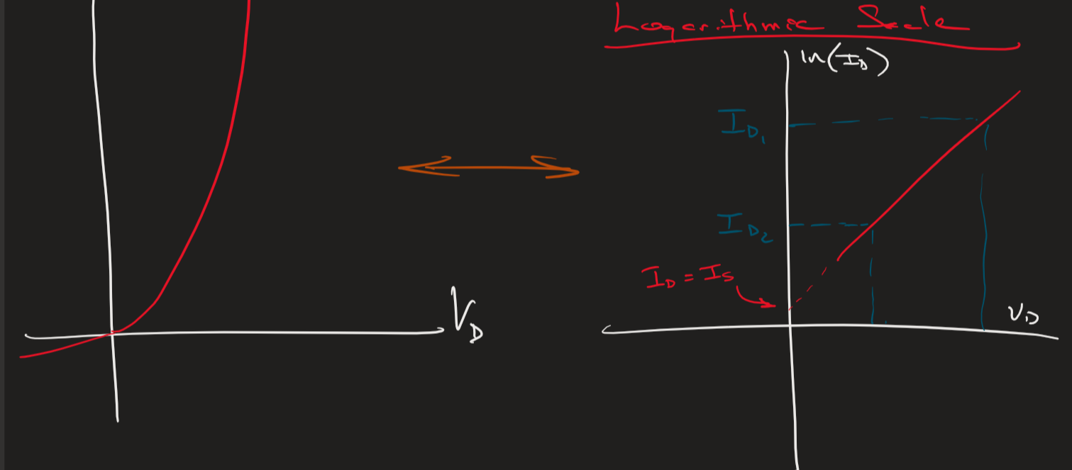
Going from the normal scale to a logarithmic scale allows us to be able to see large changes in the current for very small changes in voltage. Along with the scale advantage, we will be able to see where the value of the saturation current comes from. In order to find this value we need find the y-intercept point. It is important to note that this model is meant as an alternative to using the ideal Shockley diode equation. If you are able to get measurement data from a diode which provides at least 2 current values across the diode at specific voltage values we can use this to approximate what the Saturation current is by finding the y-intercept based on those two points. All values of this graph based on the two points are only valid greater than the threshold voltage since all voltage's less than this will have zero current (finding the y-intercept for the saturation current however is still valid). While the Shockley diode equation is a better approximation of the actual current value, the ability to know your ideality constant may be a bit more difficult, so methods such as this one can provide a alternative solution.
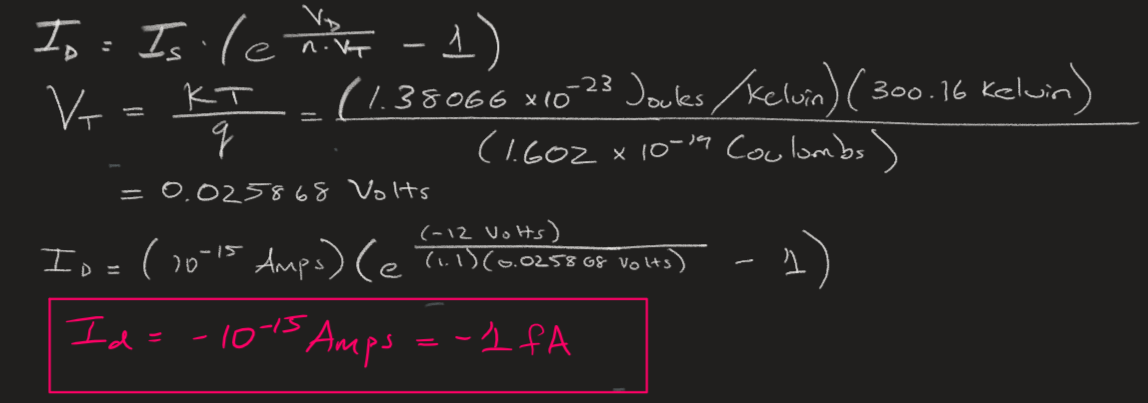
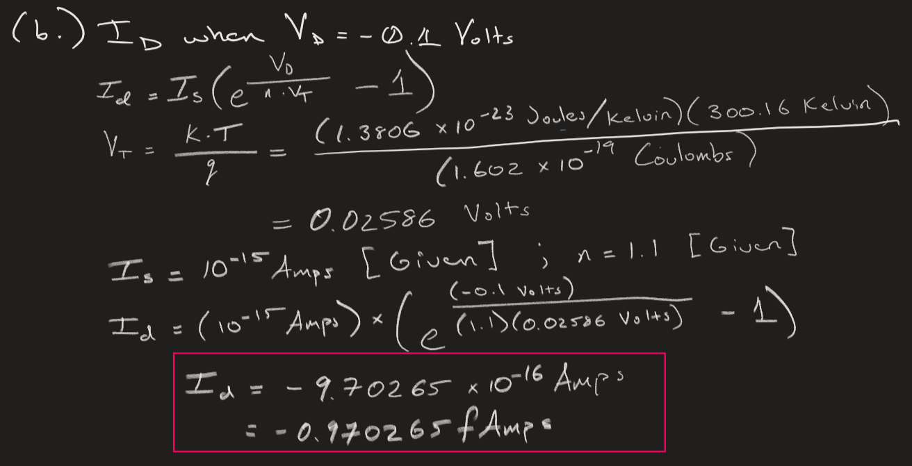
Example #1: [Attempt to do this problem by yourself before looking at the solution]
Let a diode operate at 27 degrees Celsius with a reverse saturation current of 1 fA (10^-15 Amps) and an n= 1.1
Let a diode operate at 27 degrees Celsius with a reverse saturation current of 1 fA (10^-15 Amps) and an n= 1.1
(a) Calculate Id when VD = -12V
(b) Calculate Id when VD = -0.1 V
Improved Non-Linear Models of the Diode
As we mentioned before the Shockley diode equation is great for approximating the current through a diode, but only for small currents (typically currents less than 5uA). Past 5uA those Ohmic metal contact points to the diode start to dominate the I-V curve. So in order to make our non-linear model look more realistic we will add a series resistor to our model will make our I-V curve more like that of a real life I-V curve. Here is how the VD graph changes as a result of adding the series resistor.
VD = VD ideal + ID ideal * Rseries
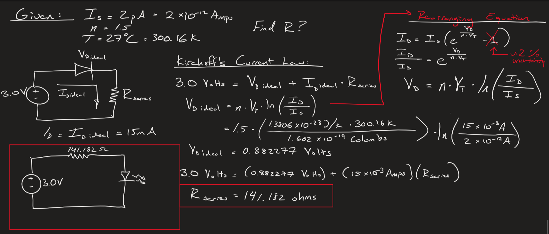
Design Specification #1: [Attempt to do this problem by yourself before looking at the solution]
Starting from a LED's manufacturer data sheet, the DC nonlinear model is: Is = 2pAa, n = 1.5, and that at least 5mA is required for visible light ligh emission. The power supply (or battery) is 3.0V and is part of a larger system constraint. Let's choose arbitrarily, after consultation with the manufacturer's datasheet, 15mA as the desired current for the intensity of the light. Design the appropriate circuit.